INTERLEAVED QUADRUPLER DC –DC CONVERTER HIGH VOLTAGE GAINWITH LOW VOLTAGE STRESS
Electrical and Electronics Project by Ravi Devani
ABSTRACT
In this paper interleaved quadrupler DC–DC converter high
voltage gain with low voltage stress. Renewable energy is important for now a
days and increases widely because of energy shortages and environmental
contaminate problem in renewable energy system generate low output voltage and
thus high step up dc-dc converter used to achieve high output voltage. In
proposed system we are using three stage interleaved boost converter ,coupled
inductor and voltage quadrupler concept used to reduced conduction losses,
voltage spikes, voltage stress , balanced output voltage and achieve high
output voltage without using extreme duty ratio and non- isolated operation.
Key words: high
step up converter, three stage interleaved converter, quadrupler and coupled
inductor and balancing capacitor.
INTRODUCTION
Nowadays, renewable energy is increasingly valued and
employed worldwide because of energy shortage and environmental contamination.
Renewable energy systems generate low voltage output, and thus, high step-up
dc/dc converters have been widely employed in many renewable energy
applications such fuel cells, wind power generation, and photovoltaic (PV)
systems. Such systems transform energy from renewable sources into electrical
energy and convert low voltage into high voltage via a step-up converter, which
can convert energy into electricity using a grid-by-grid inverter or dc micro
grid. Therefore, DC boost converter is needed to boost up a dc voltage. In dc
boost converter.
Vo =Vin*1/1-D
However a duty ratio is larger means the output voltage
is high. But the duty ratio is increasing means conduction time is high and it
will arise voltage stress on switching devices, conduction loss is high. By the
use of three interleaved stage interleaved boost converter and voltage
quadrupler concept it will achieve high output voltage and reduce voltage
stress and conduction loss.
Interleaved boost converter
Today interleaved converter is important techniques for
power factor correction design is facing many problems. Power scalability, high
power density and high entire load of efficiency. power scalability is
necessary and cost effective approaches in the power factor correction design
in that way power requirements growth is increases .The boost converter method
D duty ratio is increasing very high then only we Attain high output voltage
but the duty ratio increases means voltage stress occurs on switching devices.
The conduction losses are also very high finally the efficiency is decreases.
The filter capacitor is also added to reduce the current ripple. So the circuit
size is very high and cost is also high. They are limited possibilities is
available increasing power density due to EMI filter and increasing inductor
size. So properly choosing the duty ratio then only attains low voltage stress
and conduction losses and current ripple is also zero. The interleaved
converter properly choosing duty ratio. The conduction losses and voltage
stress is less and current ripple is also zero. The size of the circuits and
cost is also zero.
Electrical and Electronics Project by Ravi Devani
VOLTAGE QUADRUPLER
The addition of still another diode-capacitor
section to the voltage Tripler produces an output four times the peak voltage.
The circuit diagram is shown in below Figure.

Fig 1 . Voltage Quadrupler

Fig.2. Voltage Quadrupler Hardware
In such type of circuit C1 charges to Vm,
through D1, C2 charges through D2, C3 and C4 charges
through D4, C2, C3 and C4 charges to 2Vm. The 4Vm
output is taken across C2 and C4.The ripple frequency is
twice the input frequency. Theoretically there is no upper limit to the amount
of voltage multiplication that can be obtain. But practically there is a limit
the reason is that total amount of capacitance becomes large to maintain the
desired d.c. output except extremely light loads.
APPLICATION
Voltage multipliers are used in high voltage, low current applications such
as for accelerating purpose in a cathode ray tube. Generally these are used
where both the supply voltage and load are maintained constant.
BLOCK DIAGRAM
The
input is PV cell. Photovoltaic cell is a renewable energy and it is 365
available sources in tamilnadu. In a single cell voltage is 0.5V. PV panel is
connected into three stage interleaved boost converter. Interleaved boost
converter with coupled inductor. Interleaved means more than one boost
converter is connected into parallel. The output of the three stage interleaved
boost converter is connected into a voltage quadrupler .PWM controller is used
to triggering the switches.

The output of the voltage quadrupler circuit is connected
into a DC load or DC micro Grid. The work of voltage quadrupler is increasing
four times of the voltages.
CIRCUIT DISCRIPTION
The proposed system is shown in Fig 1 shows the proposed three stage
inter-leaved boost converter with coupled inductor and voltage quadrupler are
connected in the circuits two balanced capacitor are connected in the circuits
to achieve balanced output voltage. In existing system use two stage
inter-leaved circuits and voltage doublers the conduction period of two stage
inter-leaved switches used 50%.the voltage stress is high compare two proposed
system and the output of the two stage inter-leaved circuits connected to
voltage doublers circuits to achieve high output voltage. In proposed system we
are use three stage inter-leaved circuits is 33% for three switches. So it reduces
switching stress and conduction loss. The output of the three stage inter-leaved
boost converter is connected to voltage quadrupler circuit voltage quadrupler
means the output voltage is increase four times. Now we can achieved high
voltage gain .Fig. 1shows the circuit diagram of the proposed system drawn
using MATLAB simulation tool. It consists of a dc source from PV panel. Three
stage interleaved boost converter with coupled inductor and voltage quadrupler
circuits are used. The switching of the PWM inverter can be effectively
controlled by the output. The balanced capacitor is connected to achieve
balanced output voltage.

Fig.3. Proposed system inter-leaved converter
Mode.1:In
a circuit contains three switches S1,S2,S3 .In mode 1 condition switch 1 is ON
condition on that time L1,L2, L3 inductance are stored on energy. Switch 1 is
short circuit in previous mode capacitance stored energy flowing through diode
D2 after the energy is flowing to C1, C2 the load.


Fig.4.Equivalent circuit of all modes
The L2 inductance stored energy flowing through diode D4
and D6 through the load. The L3 inductance stored energy flowing through diode
D5 and d7 through the load. The coupled inductance is used in the
circuits so the energy is increasing twice the times it’s flowing to C4, C1 and
C2 capacitor. Balancing capacitor C1, C2 is used in the circuit to achieving
balanced output voltage.
Electrical and Electronics Project by Ravi Devani
Mode2: In mode
2 condition switch 2 is ON condition on that time L1, L2, L3 inductance are
stored on energy. In previous mode switch 1 is OFF condition. Switch 2 is short
circuit in previous mode capacitance stored energy flowing through diode D7 to
the load. The L1 inductance stored energy flowing through diode D1 and D7
through the load. The L3 inductance stored energy flowing through diode D5 and
d7 through the load. The coupled inductance is used in the circuits so the
energy is increasing twice the times it’s flowing to C4, C1 and C2 capacitor.
Balancing capacitor C1, C2 is used in the circuit to achieving balanced output
voltage.
Mode 3: In mode
3 condition switch 1 is ON condition on that time L1, L2, L3 inductance are
stored on energy. In previous mode operation switch 2 is OFF condition. Switch
3 is short circuit in previous mode capacitance stored energy flowing through
diode D5 and d7 to the load. The L1 inductance stored energy flowing through
diode D1 and D7 through the load. The L2 inductance stored energy flowing
through diode D4 and D6 through the load.The coupled inductance is used in the
circuits so the energy is increasing twice the times it’s flowing to C4, C1 and
C2 capacitor. Balancing capacitor C1, C2 is used in the circuit to achieving
balanced output voltage.
SIMULATION RESULTS AND DISCUSSION
The proposed converter 18-v input voltage and 158-v output voltage fig 1 is
chosen. The switching frequency is used in the circuit is 50 kHz, the duty
ratio of S1, S2, S3 is 0.33 so it is used to reduce voltage stress and current
stress and finally it reduce conduction losses. The output voltage is increases
up to 158v after it attains transient states on time period 0.6sec. The
conduction losses on state voltage reaches attain 0.1-v the conduction of
current is 6.85A.The duty ratio timing period is o.33.

Fig.5. Proposed input voltage
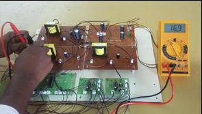
Fig.6. Proposed hardware input voltage

Fig.7. Hardware output voltage

Fig8. Output voltage and current
Conduction losses for proposed system
i/p voltage =17 v
o/p voltage =158v
power = V*I=158*3.165
P = 500.07W
Pon = Von Io Ton
Von = on-state voltage
Io = conducting of current
Ton = conduction during the ON time interval
Pon = 0.1*6.8*0.33
Pon = 0.224W
CONCLUSION
In this paper interleaved quadrupler voltage DC-DC
converter was discussed and it has achieved high voltage gain and reduced
voltage stress, current ripple and conduction losses with the help of three
stage inter-leaved boost converter with voltage quadrupler circuits and to get
a balanced output voltage connection of balanced capacitor finally the input
voltage is 18v and the output voltage is 158v. The conduction losses is 0.224w
for 500.07w power.
REFERENCES
1.B. R. Lin and F. Y. Hsieh, Soft-switching Zeta–Flyback
converter with a buck–boost type of activeclamp, IEEE Trans. Ind. Electron.,
54(5), 2007, 2813–2822.
2.C. M. Wang, A novel ZCS-PWM flyback converter with a
simple ZCS PWM commutation cell, IEEETrans. Ind. Electron, 55(2), 2008,
749–757.
3.Ching-Tsai Pan, Member, IEEE, Chen-Feng Chuang, and
Chia-Chi Chu, Member, IEEE, ANovel Transformer-less Adaptable Voltage
Quadrupler DC Converter with Low Switch Voltage Stress. IEEEtransactions on
power electronics, 29(9), 2014.
4.E. H. Ismail, M. A. Al-Saffar, A. J. Sabzali, and A. A.
Fardoun, A family of single-switch PWMconverters with high step-up conversion
ratio, IEEE Trans. Circuits Syst. I, Reg. Papers, 55(4), 2008, 1159–1171.
5. F. Zhang, L. Du, F. Z. Peng, and Z. Qian, A new design method
for high power high-efficiencyswitched-capacitor DC–DC converters, IEEE Trans.
Power Electron., 23(2), 2008, 832–840.
6.J. M. Kwon and B. H. Kwon, High step-up active-clamp
converter with input-current doubler and output voltage doubler for fuel cell power
systems, IEEE Trans. Power Electron., 24(1), 2009, 108–115.
7.Kuo-Ching Tseng and Chi-Chih Huang, High Step-Up
High-Efficiency Interleaved ConverterWith Voltage Multiplier Module for
Renewable Energy System, IEEE transactions on industrial electronics, 61(3),
2014, 1311-1319.
8.L. Zhu, A novel soft-commutating isolated boost
full-bridge ZVS-PWM DC–DC converter forbidirectional high power applications,
IEEE Trans, Power Electron., 21(2), 2006, 422–429.
9.N. P. Papanikolaou and E. C. Tatakis, Active voltage
clamp in flyback converters operating in CCM modeunder wide load variation,
IEEE Trans. Ind. Electron., 51(3), 2004, 632–640.
10.Q. Zhao and F. C. Lee, High-efficiency, high
step-upDC–DCconverters, IEEE Tran s. Power Electron., 18(1), 2003, 65–73.
11.R. J. Wai and W. H. Wang, Grid-connected
photovoltaic generation system, IEEE Trans. Circuits Syst.I, Reg. Papers,
55(3), 2008, 953–964.
12.R. J. Wai, W. H. Wang, and C. Y. Lin,
High-performance stand-alone photovoltaic generation system, IEEE Trans. Ind.
Electron., 55(1), 2008, 240–250.
13.W. Li and X. He, Review of non-isolated high
step-up DC/DC converters in photovoltaic grid-connectedapplications, IEEE
Trans. Ind. Electron., 58(4), 2011, 1239–1250.
Electrical and Electronics Project by Ravi Devani
No comments:
Post a Comment