Blog Archive

Wednesday, 28 December 2016

MICRO CONTROLLER BASED AC POWER CONTROLLER

MICRO CONTROLLER BASED AC POWER CONTROLLER
ABSTRACT
This paper discusses the design and implementation of single phase PWM inverter using 8051 microcontroller. The main features of 8051 based PWM inverter are simpler design, low cost, maximum range of voltage control and compact in size. The designed PWM inverter is tested on various AC loads like AC motor and intensity control of incandescent lamp in a closed loop environment.
Keywords: Gate Signals Generation, Micro Controller, Pulse Width Modulation, PWM Generation

INTRODUCTION
The pulse width inverters can be broadly classified as  
(1) Analog bridge PWM inverter
(2) Digital bridge PWM inverters
The advantage of Analog based PWM inverter controller is that, the level of inverter output voltage can be adjusted in a continuous range and the throughput delay is negligible. The disadvantages of Analog based PWM inverters are:
Analog component output characteristics changes with the temperature and time. They are prone to external disturbances. Analog controller circuitry is complex and bulky. They are non-programmable, hence not flexible.
On the other hand Microcontroller based PWM inverter controller (Digital bridge PWM inverter) makes the controller free from disturbances and drift, but the performance is not very much high due to its speed limitation. However to minimize throughput delay, some microcontroller based PWM inverters, retrieves switching patterns directly from memory so that calculation can be minimized, but this technique demands more memory. This drawback can be eliminated if switching pat-terns are generated by executing simple control algorithms. Even after using simple control algorithms, sometimes throughput delay may be substantial.
With the availability of advanced microcontrollers and DSP [Digital signal processor] controllers, with many advanced features like inbuilt PWM generator, event managers, time capture unit, dead time delay generators, watch dog timers along with high clock frequency, the limitation of speed, associated with microcontroller based PWM inverters can be neglected to some extent.
This paper presents a simple and cost effective technique of implementing single-phase AC [alternating current] voltage controller, used to control AC loads, which doesn’t demand very high precisions, using 8051 micro-controller.

PWM BRIDGE INVERTER REVIEW
Inverters can be classified as single-phase and three phase inverters and they are further classified as Voltage fed inverter [VSI.], current fed inverter [CFI], and variable DC [direct current] linked inverter. In Volt-age fed inverter, input voltage remains constant, in cur-rent fed inverter [CFI], input current remains constant and in variable DC [direct current] linked inverter, input voltage is controllable.
 
Figure 1. Single phase inverter.
 
Figure 2. O/P voltage/gate signals.
Figure 1 shows single phase bridge inverter with MOSFET switches. In spite of MOSFET switches having high ON state resistance and conduction losses, in this paper MOSFET switches are used because of the following reasons. MOSFET being a voltage con-trolled device, it can be driven directly from CMOS or TTL logic and the same gate signal can be applied to diagonally opposite switches. Also the gate drive current required is very low.
The working principle of Single-phase bridge inverter can be explained as follows.
Positive Voltage ‘Vs’ appears across the load, when MOSFET Q1 and Q2 conduct simultaneously. Negative voltage ‘Vs’ appears across the load, when Q3 and Q4 conduct simultaneously.
To overcome the effect of back emf in case of inductive load diodes, D1-D4 are used. Diode D1 and D2 are called feedback diodes, because when they conduct the energy is feedback to the DC source. The RMS output voltage is given by
where P is pulse width. The O/P voltage and gate signals are as shown in Figure 2.
CONTROLLER BLOCK DIAGRAM
The block diagram of microcontroller based bridge PWM inverter is as shown in Figure 3. The required four digit speed in RPM [Rotation per Minute] is entered through the keyboard and corresponding to the key pressed, digital equivalent of that RPM is stored in memory.
Current running speed of the AC motor is sensed through speed sensor, and the analog output given by the sensor is converted to digital data using Analog to Digi-tal converter [ADC].
 
Figure 3. Block diagram of controller.
 
Figure 4. Flowchart of basic operation.
 
Figure 5. Flow chart of keyboard logic.
 
Figure 6. Flowchart of keyboard logic.
 
Figure 7. Flowchart of A/D converter.
The digital data is accepted through 8051 microcontroller ports and is compared with required speed’s equivalent digital data. In accordance with the error signal, the width (duty cycle) of PWM signal is varied, which in turn controls the AC voltage.
From the generated PWM signal, required two gate signals are generated using external interrupt to drive the bridge inverter circuit.
Gate signals are boosted up to a sufficient voltage level by using gate driver circuit, so that it can drive the MOSFET switches of bridge inverter to the ON state. User can alter the speed at any instant of time in accordance to his requirements. Many additional features can be further added like sensing the temperature of room and automatically controlling either the speed of the fan or the level of air conditioning required. Figure 4 explains the logic flow of the basic operation.

CONTROLLER DESIGN
Controller is designed by using simpler low cost components like 8051 microcontroller, 8 or 12 bit Analog to Digital Converter (ADC), 4×4 keypad, 4 chopper MOS-FET switches (IRFZ48) and speed/Intensity sensor.
The controller design can be explained under 4 sections as:

Keypad Interface
A 4×4 keypad is interface with 8051 microcontroller as shown in Figure 5, through which four keys are accepted.
After accepting the four keys they are combined to rep-resent four digit required RPM, which actually represents the external memory address, in which digital equivalent of speed is stored.
For example if the keys entered are 1 (01), 2 (02), 3 (03), 4 (04), then they are combined as 1234 (RPM), which represents External memory address, in which 8 bit digital equivalent of that speed is stored. Higher byte of the memory address is stored in DPH [data pointer high byte]. Lower byte of the memory address is stored in DPL [data pointer low byte]. This method saves time since it doesn’t require any program execution to convert the entered speed in RPM into its digital equivalent. The other method is to enter equivalent digital data of RPM directly, provided a conversion chart is available [external look-up table]. This technique will save some memory access time, since communication with memory is avoided.

ADC Interfacing
Whenever speed varies from zero to maximum, the speed sensor O/P varies from zero to five volts respectively. An 8-bit ADC with resolution 1/28 is used to convert the analog voltage to digital data. Minimum of 19.5 mv change in voltage (corresponding change in RPM) is required to change the digital state of ADC. This limits the accuracy of the application. The logic of interfacing ADC is as explained in the flowchart given in the Figure 7.

PWM Generation
8051 microcontroller do not have on-chip PWM generator. It is implemented using ‘A’ register and any other register (R0-R7) as shown in Figure 8.
A count (ON period time) is loaded onto one of the GPR (General purpose register), which can be called as Duty cycle register and accumulator (‘A’) is loaded with zero. Register ‘A’ is incremented in steps of one and continuously compared with duty cycle register.
 
Figure 8. PWM generation.


Figure 9. Gate signal generation using interrupt.


Figure 10. Gate signal booster circuit.


Figure 11. Response for various loads with corresponding duty cycles.

If the ‘A’ contents are less than duty cycle register, high level is maintained at port line P1.1. When ‘A’ is higher than duty cycle register content a low level is maintained on port line. The alternate technique is to use Timer as Counter by applying clock pulses externally and comparing the count present in the counter with ‘A’ register (duty cycle register). This demands external clock source, since 8051 do not have any clock out pin.
Since the maximum time period is limited to 256 microseconds, the minimum frequency of PWM signal will be 4 KHz, but this can be changed using software delays. The AC signal frequency generated by PWM bridge inverter depends on PWM signal frequency. The error signal is generated by comparing the required speed with accepted digital equivalent speed divided by two. In proportionate with the error signal, PWM duty cycle is varied. When the required speed value is less than the accepted one, duty cycle register value and accepted value is decremented by one continuously till accepted value is equal to the required speed’s digital value. When the required speed value is more than the accepted one, duty cycle register values and accepted value is incremented by one continuously till accepted value is equal to the required speed digital values.

Gate Signal Generation
The generated controlled PWM signal itself will be one set of gate signal (g1, g2) and other set of gate signals (g3, g4) is generated using interrupt technique. The controlled PWM signal generated is given to the external interrupts, which is initialized as falling edge sensitive interrupt type. When controlled PWM signal’s falling edge occurs, an interrupt service routine meant for that particular external interrupt is executed.
In the interrupt service routine, a delay is created equal to the time, 7FH minus duty cycle register content, after which, the port line is made high and is retained high for the time duration decided by the contents of duty cycle register (Figure 9).
The gate signal (vg1 vg2, vg3, vg4) are boosted to a sufficient voltage level by Gate drive circuitry as shown in Figure 10, so that they are capable of driving MOS-FET’S to the ON state, when the gate signals are high.
A transistor switch (with inverted gate signals as in-put) is made used to boost the gate signal. The same DC supply, which is used for inverter is also used to drive the transistor by reducing the DC level using voltage dividers. The other technique is to use opto isolators. Both of these techniques use the same inverter DC source to boost up the gate signals, thus avoiding more usage of DC sources.

RESULTS AND CONCLUSIONS
The designed application is tested by designing 60V MOSFET bridge inverter.
Harmonics are removed by using simple capacitor filter and the AC voltage is stepped up to 220 V using step-up transformer. The performance of application is tested on various A.C loads and the plots of the same are as shown in Figure 10. The design exhibits good results for the load values of 50 ohm and 100 mH/ 10mH. A simple PWM technique with 100% duty cycle variation, which reduces hardware and software complexity, is used rather than using the most often used complex sinusoidal PWM technique (For Single-phase inverters). Required dead time is generated through interrupt, which avoids the usage of dead time delay generators. With minor modifications the same work can be used to control light intensity, temperature etc., The accuracy can be further improved by using high resolution ADC’s and the delay involved in the software can be overcome using higher versions of controllers.

REFERENCES
(1) H. Parasuram and B. Ramaswami, “A three phase sine wave reference generator for thyristorized motor control-lers,” IEEE Transactions on Industrial Electronics, Vol. IE-23, pp. 270–276, August 1976.
(2) J. M. D. Murphy, L. S. Howard, and R. G. Hoft, “Micro-processor control of PWM inverter induction motor drive,” in Record of the 1979 IEEE Power Electron Spe-cialist Conference, pp. 344–348.
(3) G. S. Buja and P. Fiorini, “Microcomputer control of PWM inverters,” IEEE Transactions on Industrial Elec-tronics, Vol. IE-29, pp. 212–216, August 1982.
(4) G. S. Buja and P. De Nardi, “Application of a signal processor in PWM inverter control,” IEEE Transactions on Industrial Electronics, Vol. IE-32, No. 1, February 1985.
(5) Y. K. Peng, et al., “A novel PWM technique in digital control,” IEEE Transactions on Industrial Electronics, Vol. 54, February 2007.
(6) M. H. Rashid, “Power Electronics Circuits, Devices and Applications,” 3rd Edition, Prentice-Hall of India, Private limited, New-Delhi, 2004.
(7) V. Jagannathan, “Introduction to power electronics,” Prentice-Hall of India, Private limited, New-Delhi, 2006.


HIGH VOLTAGE GENERATION BY USING COCKCROFT-WALTON MULTIPLIER

HIGH VOLTAGE GENERATION BY USING COCKCROFT-WALTON MULTIPLIER
ABSTRACT
In this paper present High Voltage DC generation by using Cockcroft-Walton Multiplier are purpose. This section is providing continues input current, with a low ripple cascading of diode and capacitor. Cockcroft-Walton multiplier provide suitable high DC voltage source from a low input voltage i.e, 230V AC supply which is rectified by using half wave rectifier circuit. Cockcroft-Walton multiplier constructed by ladder network of capacitor and diode for generation of high voltage. When number of stages of multiplier are increase output of the Cockcroft-Walton Multiplier is also increasing. In this paper 8 stages Cockcroft-Walton multiplier are use to generated high voltage. In this paper transformer method are eliminated therefore cost and size of Cockcroft-Walton multiplier are reduce. Other specifications considered carefully while designing multiplier and components must be used based on size consideration for expected load current and expected output voltage. A prototype was designed and experimental result was tested and demonstrate was purpose.
Key words - Cascading circuit, Cockcroft-Walton multiplier, High voltage, Voltage divider.

INTRODUCTION
High voltage generation DC power is widely used in the research work and industry level. It is also used in the scientific instrument, TV sets and CRTs, Oscilloscope, x-ray and photomultiplier tubes are used in nuclear industry for detection of radiation. The method stepping up the voltage is commonly done by a step-up transformer. The output of the secondary of the step up transformer increases the voltage and decreases the current and losses occurred in the transformer is more this is for case of AC system. But in DC system transformer are not in used because of the constant current in case of DC system and hence, constant flux which is not link primary to secondary and therefor transformer method are eliminated in the case of DC. For stepping up the voltage in DC system multiplier method are prefer. Multipliers are primarily used to develop high voltages where low voltage at the input side. In this section describes the concept to develop high voltage DC from a single phase AC ie. 230 Volt, 50 Hz system. Because of the safety consideration it was restricts the multiplication factor to 8 such that the output would be within 1KV. The design of the circuit involves Cockcroft-Walton multiplier, whose principle is to go on doubling the voltage for each stage. Thus, the output from an 8 stage voltage multiplier can generate up to 1KV.

COCKCROFT-WALTON MULTIPLIER
The Cockcroft-Walton is a voltage multiplier that converts AC or pulsing DC electrical power from a low voltage level to a higher DC voltage level. It is made up of a voltage multiplier ladder network of capacitors and diodes to generate high voltages. Unlike transformers, this method eliminates the requirement for the heavy core and the bulk of insulation/potting required. Using only capacitors and diode in cascading network these voltage multipliers can step up relatively low voltages to extremely high values, while at the same time being far lighter and cheaper than transformers.
 
Fig -1: Cockcroft-Walton multiplier
Where, C1,C2,C3…..Cn= Capacitor ,
D1,D2,D3…Dn =Diode, And 
ID1, ID2, ID3, ….. ID1 =Diode Current. 
The advantages of Cockcroft-Walton Multiplier circuit are low in cost, small in size and can be easy to insulate the circuit.
Another advantage of voltage of multiplier circuit is its peak to peak voltage at each stage will be double.
Consider operation of two stages Cockcroft-Walton multiplier is shown in figure1.
1) When TS is negative, then Capacitor C1 charges through Diode D1 to Vmax.
2) When Ts is positive, then Vmax add arithmetically existing potential C1, thus C2 charges to 2Vmax through D2.
3) Again Ts is negative, C3 charge 2Vmax through Diode D3.
4) Again Ts is positive, Capacitor C4 charge Diode D4 to 4Vmax.
Therefor output of multiplier = Vmax * N
Where,
N = Number of stages.
Designing of Multiplier circuit most commonly half wave circuits are used. And because of the multiplier circuit, high voltage develop at the output side of the Cockcroft-Walton multiplier circuit.
Design of Cockcroft voltage multiplier is simple Careful consideration of all component parameters is the only way to insure both reliable and predictable circuit performance.[2]
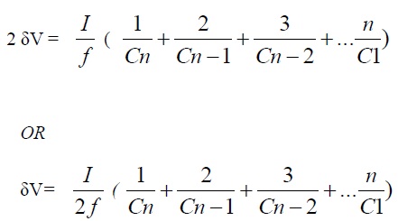
Ripple of the n-stage multiplier will be,
 ............(1)
from equation (1) it is clear that, multistage circuit the lowest capacitors are responsible for most ripple and it is, therefore, desirable to increase the capacitance in the lower stages.
Therefore, capacitors of equal value are used in practical circuits i.e., Cn = Cn – 1 = ... C1 = C and the ripple is given as,
 
The second quantity to be evaluated is the voltage drop ΔV which is the difference between the theoretical no load voltage 2nVmax and the onload voltage.
Voltage drop ΔV = (I/fc) (2/3 n³ + n²/2-n/6) 
Regulation of voltage = V/2nEm,
Ripple (%) = δV/2nEm

RIPPLE VOLTAGE
Ripple voltage is the magnitude of fluctuation in DC output voltage at a specific output current (assuming AC input voltage and AC input frequency are constant). A close approximation for series half-wave multipliers can be expressed as:
VRIP = I(N2+N/2)/8FC
Example: Calculate the ripple voltage of a 6 stage multiplier with 1000pF capacitors, 50kHz input frequency (sine wave), 1mA DC output current, 20kV DC output voltage:
VRIP = (1*10-3(62+6/2))/8*50000*(1*10-9))
VRIP = 97.5Vp-p

DESIGN AND TEST SETUP
For the application of various equipment in 8 stages Cockcroft-Walton multiplier designed with a multiplication of peak to peak voltage ie. N * Vmax at a last stages of Cockcroft-Walton multiplier.
 
Fig -2: Block diagram of test setup
A voltage divider is used for deviation of voltage with a very high resistance. The two main components are used in the setup as shown.in figure 2. They are amplifier and 8 stages voltage multiplier. Amplifier is used to amplify the DC input signal and 8 stages Cockcroft-Walton multiplier is used to step up DC voltage into a high voltage at 1KV or 1000 Volt  from 230 V AC voltage which rectified and convert in AC-DC. Voltage adjuster is used to adjust the voltage and amplifier end for supplying to the Cockcroft-Walton multiplier circuit. The operation of a multiplier is to be effectively multiplying the peak to peak voltage by number of stages and convert into high voltage. The voltage at the 1st stage of multiplication is 120V DC. The voltage at the 8th stage of multiplication is 960VDC. In theoretical consideration these values were somewhat reduced because of losses in the diodes, capacitances and leakage currents of the diodes, component tolerances of the diodes and capacitors, etc. The voltage divider in which high value of resistance are use. In the actual prototyped circuit, we used 10 Mohm resistors because of availability in the experiment. Components are used in prototype model Capacitor and Diode in cascade network, and operational amplifier (741). In figure 3. Shows that if the output voltage of a Cockcroft-Walton multiplier is increase according to number of stages. In theoretically at first stages output is 120 peak to peak voltage and at the end of 8 stages the peak to peak voltages is 960 volt. Developed high voltage D.C. Power supply based on Cockcroft-Walton voltage multiplier circuit. This circuit is a unique circuit which is developed for the special applications like field testing of high voltage cables, prime D.C. voltage. Construction of multiplier circuit is simple in nature because, it is cascading of diodes and capacitors which is low cost component this is the advantages of multiplier circuit and it also required less insulation from last stages of the voltage multiplier circuit.
 
Fig -3: Characteristics of output voltage and number of stages

CAPACITOR AND DIODE SELECTION
While designing multiplier and capacitor and diode must be used based on size consideration for expected load current and expected output voltage. Range of capacitor is commonly 1 microfarad to the 250 microfarad, whose voltage rating is usually twice that of actual peak to peak voltage. For example a capacitor which will see a peak voltage of 2Vmax should have a voltage rating of approximately 4Vmax. For selection of diode, parameter must be consider. When the maximum reverse voltage across a diode that is known as peak inverse voltage. This peak reverse voltage are available in each diode therefor for selection of diode rating which is 2 * Vmax for a safety purpose.

CONCLUSION
The Cockcroft-Walton Multiplier surface mount and design in which high voltage generate without use transformer is a beauty of the high voltage Cockcroft-Walton circuit. There for size of the complete high voltage circuit is small and cost is also less. This small size circuit gives high voltage at the end of multiplier circuit. Because of the light weighted circuit it is portable it gives high reliability. Construction of whole circuit is simple and robust in nature. This multiplier circuit is useful for a scientific instrument, TV sets and CRTs, Oscilloscope, x-ray and photomultiplier tubes and field testing of HV cables.

EXPERIMENTAL SETUP
In this experiment used 1 to 250 microfarad capacitor are used and IN 4007 Diode which is cascading in the Cockcroft-Walton multiplier circuit. Digital multimeter which is used to measure the High Voltage at the end of multiplier circuit.
 
Fig -4: Prototype setup of Cockcroft-Walton multiplier circuit

REFERENCES
[1]. D. F. Spencer, R. Aryaeinejad, E. L. Reber," Using the Cockcroft-Walton Voltage Multiplier Design in Handheld Devices”, INEEL/CON-01-01424 PREPRINT October 2001.
[2]. C. K. Dwivedi ,M. B. Daigavane," Multi-purpose low cost DC high voltage generator (60 kV output), using Cockcroft-Walton voltage multiplier circuit‖, International Journal of Science and Technology Education Research Vol. 2(7), pp. 109 - 119, July 2011.
[3]. G.S. Senthil Raaj, G.T. Sundar Rajan," Simulation and Implementation of Single-Phase Single-Stage High Step-Up AC–DC Matrix Converter based of Cockcroft–Walton Voltage Multiplier‖, International Conference on Innovations In Intelligent Instrumentation, Optimization And Signal Processing “ICIIIOSP-2013”
[4]. Cheeru G. suresh, Elizabedh Rajan,Chittesh V.C.,Chinnu G. suresh," Transformless high step-up DC-DC Cockcroft-Wolton multiplier in hybrid system‖, IRF International Conference on 10th August 2014, Cochin, India, ISBN: 978-93-84209-43-8
[5]. Nileena P. Subhash, Ajmal K.A, K. Punnagai Selvi," A High Step-Up Converter Using Transformerless Cockcroft-Walton Voltage Multiplier for a PV System,‖ International Conference on Engineering Technology and Science-(ICETS’14)
[6]. Adinath Jain, Simith E," AC-DC Matrix Converter Based On Cockcroft-Walton Voltage Multiplier‖, IOSR Journal of Engineering (IOSRJEN), Vol. 04, Issue 07 (July. 2014). PP 16-23
[7]. Naidu MS, Kamaraju V (2004),‖High Voltage Engineering‖, Third Edn. McGraw- Hill Company Ltd. pp. 146-156
[8]. C. L. Wadhwa, ―High Voltage Engineering‖.New Age International Publication. pp. 56-63.

Thursday, 22 December 2016

taimur ali khan

taimur ali khan
why controversy to west the time???


In most human cultures, the birth of a child is an unambiguously happy event. This moral framework does not, it seems, apply to some sections of social media, where for the most part of Tuesday, Tweeters bemoaned the birth of a new Bollywood baby. Born to A-list film stars, Saif Ali Khan and Kareena Kapoor, the boy had been named Taimur – a highly objectionable christening for some, given the name’s association with a 14th century Turkic king and one the world’s most successful conquerors.
What was wrong with Taimur? Social media users were ostensibly objecting to the brutal nature of his conquests. Of particular concern was Taimur’s campaign against his fellow Turkics, the Tughlaq Sultanate of Delhi. Conducted in 1398, the Timurid invasion eventually led to the sack of Delhi city where, by some accounts, the entire population of the city was massacred.
So deeply felt was this sack that 700 years later, Indians on Twitter would call the new-born baby a “terrorist”, a “jihadi” and in general wish harm upon it.

While it may be easy to dismiss this as the work of trolls, the frankness of social media provides us an important window to attitudes that might otherwise not be aired publicly. With Hindutva in the ascendant, this incident shines a bright light upon how India’s medieval age is treated with a mixture of ignorance and paranoia by those who follow this ideology. Hindutva pushes a narrative of ahistorical Muslim rule and then, is the first victim of its own misrepresentation. This distorted image of Muslim conquests projected by Hindutva creates a deep inferiority complex right at its centre. So much so that it was eventually expressed as tragi-comic social media rage against a day-old infant.
Heroes and villains
Historical narratives are tricky things to construct, especially when people want to superimpose moral lessons on them. Who is a hero and who isn’t is extremely subjective and even more so when one goes as far back in time as the 14th century. The past truly is a different country and to make it fit modern standards of morality, a fair bit of invention needs to be indulged in.
Let’s take a force that is near-universally seen as the “good” guys in popular Indian history: the Marathas. The Marathas were successful towards the end of the Mughal period, building up a confederation over large parts of the subcontinent. Of course, this was done through war and conquest and in the chaos of the Mughal twilight, contemporary accounts of the Marathas are often rather negative, cutting across what we would today see as “Hindu” and “Muslim” sources.
In the 18th century, the Marathas invaded Bengal killing, by one account, four lakh Bengalis. Repeated raids and conquests of neighbouring Gujarat were also, as almost everything in medieval India, a rather violent affair. In another case, Maratha armies raided a thousand-year old Hindu temple to teach Mysore sultan Tipu Sultan – who was its patron – a lesson. The Brahmin Peshwa rulers of the Maratha state enforced untouchability so brutally that BR Ambedkar actually saw their defeat at the hands of the British to be a blessing.
Contemporary accounts of the Marathas in Bengal are obviously far from flattering. Similarly, as late as 1895, there were strong objections in Gujarat to the plans of Bal Gangadhar Tilak to institute a Shivaji festival across India, with the Deshi Mitra newspaper of Surat disparaging it as a “flare up of local [Marathi] patriotism”.
India’s medieval period did not have the sort of nationalisms and community mobilisation that modern India would see under the Raj. As newspapers and technology knit the peoples of India together, a Hindu consciousness would revise the image of the Marathas as “Hindu”. Calcutta city’s intelligentsia at the time, in fact, celebrated a Shivaji festival and the city still has statues of Shivaji. Gujarat, where Hindutva has been a powerful political force for decades now, has adopted Shivaji with even more gusto, building statues in cities like Surat, which, ironically, were sacked by the Maratha chief early on in his career. This confusion is nothing new. Today, Punjabi Muslims in Pakistan see themselves as inheritors of the Mughals but in 1857 signed up enthusiastically for the East India Company’s armies to defeat the Mughal-led revolt against the Raj.
That which we call a rose
Naturally, then, the name Shivaji or Bhaskar – a Bhaskar Pandit led the Maratha raids on Bengal – are hardly taboo in modern India given this modern narrative of the Marathas.
It is the same for other names as such Ashoka or Alexander, both of whom led bloody campaigns but are common names among the supposed peoples they conquered. Sikandar, the Persian version of Alexander, is a common name across Iran and the subcontinent – a Bharatiya Janata Party parliamentarian’s son is, in fact, named after the Macedonian conqueror. Moreover, one would assume Ashoka carries no particular taboo in Orissa in spite of the Kalinga war.
In fact, this linking of a name to a supposed historical villain is a particularly egregious example of just how puerile Hindutva can be. It is a bit silly to think that someone would be outrage over the fact that a baby is named Joseph just because of Stalin’s role in the Soviet Union or “Manu” would be taboo simply because he was supposed to have authored the castiest Manu Smriti, a book of law linked to India’s crippling 2,000 year old system of caste apartheid.
This near-comical understanding of history, though, is not a new thing for Hindutva. The ideology has built a curious understanding of India’s medieval period, which it sees primarily through the lens of supposed invasions by Muslim kings and emperors. The founder of Hindutva, Vinayak Savarkar would, for example, even use this grievance to validate modern wrongs – in one case justifying the use of rape as a political tool. Prime Minister Modi, a lifelong member of the Rashtriya Swayamsevak Sangh, has often claimed India has suffered from 1,200 years of slavery.
Inventing an inferiority complex
This rage is, of course, large ahistorical. Taimur, for example, finds little mention in historical works written by Hindus at the time or even hundreds of years after. In fact, his negative image is taken solely from Muslim writers, given that his brutal invasions were led almost exclusively against Islamic empires such as the Ottomans and the Mamluks of Egypt and Syria. Ironically, even in India, his invasion targeted what Hindutva would characterise as a Muslim and therefore “foreign” dynasty, the Tughlaqs.
However, the invention of this distorted history has has a rather deleterious effect on the Hindutva mind. Tales of a “thousand years of slavery”, as one could very well imagine, create a sort of mass inferiority complex. Even in this case, for example, as important a driver of rage as the name “Taimur” was, almost as significant was the incipient anger at the fact that a Hindu woman, Kareena Kapoor, had married a Muslim man. The shadow of so-called love jihad, which once was a Bharatiya Janata Party policy position itself, only ends up harming Hindu women, given that it assumes they themselves aren’t free to make their own choices, romantic or otherwise.
This mass self-flagellation, a near masochistic nurturing of grievance, produces a highly distorted modern politics, showing how far Hindutva is from assuming any mantle of intellectual leadership, in spite of capturing political power at the federal level in India. An ideology that needs to pick on a little baby to prove its spurs has a long way to go before it can sit at the high table.

Dr Neelakshi Goswami @DrNeelakshiGswm
Hindu girls shld learn frm Kareena, think before u speak & look before u marry. Or else ur kids will be Chengiz Khan, Aurangzeb & Taimur.


Final point. If this controversy forces some Hindutava ideologues to pick up a book and read the history of Taimur, we might be in for another storm. Taimur’s heir and the next ruler of the Timurid dynasty was a man named, well, Shah Rukh.