Blog Archive

Showing posts with label mini projects. Show all posts

Wednesday, 28 December 2016

HIGH VOLTAGE GENERATION BY USING COCKCROFT-WALTON MULTIPLIER

HIGH VOLTAGE GENERATION BY USING COCKCROFT-WALTON MULTIPLIER
ABSTRACT
In this paper present High Voltage DC generation by using Cockcroft-Walton Multiplier are purpose. This section is providing continues input current, with a low ripple cascading of diode and capacitor. Cockcroft-Walton multiplier provide suitable high DC voltage source from a low input voltage i.e, 230V AC supply which is rectified by using half wave rectifier circuit. Cockcroft-Walton multiplier constructed by ladder network of capacitor and diode for generation of high voltage. When number of stages of multiplier are increase output of the Cockcroft-Walton Multiplier is also increasing. In this paper 8 stages Cockcroft-Walton multiplier are use to generated high voltage. In this paper transformer method are eliminated therefore cost and size of Cockcroft-Walton multiplier are reduce. Other specifications considered carefully while designing multiplier and components must be used based on size consideration for expected load current and expected output voltage. A prototype was designed and experimental result was tested and demonstrate was purpose.
Key words - Cascading circuit, Cockcroft-Walton multiplier, High voltage, Voltage divider.

INTRODUCTION
High voltage generation DC power is widely used in the research work and industry level. It is also used in the scientific instrument, TV sets and CRTs, Oscilloscope, x-ray and photomultiplier tubes are used in nuclear industry for detection of radiation. The method stepping up the voltage is commonly done by a step-up transformer. The output of the secondary of the step up transformer increases the voltage and decreases the current and losses occurred in the transformer is more this is for case of AC system. But in DC system transformer are not in used because of the constant current in case of DC system and hence, constant flux which is not link primary to secondary and therefor transformer method are eliminated in the case of DC. For stepping up the voltage in DC system multiplier method are prefer. Multipliers are primarily used to develop high voltages where low voltage at the input side. In this section describes the concept to develop high voltage DC from a single phase AC ie. 230 Volt, 50 Hz system. Because of the safety consideration it was restricts the multiplication factor to 8 such that the output would be within 1KV. The design of the circuit involves Cockcroft-Walton multiplier, whose principle is to go on doubling the voltage for each stage. Thus, the output from an 8 stage voltage multiplier can generate up to 1KV.

COCKCROFT-WALTON MULTIPLIER
The Cockcroft-Walton is a voltage multiplier that converts AC or pulsing DC electrical power from a low voltage level to a higher DC voltage level. It is made up of a voltage multiplier ladder network of capacitors and diodes to generate high voltages. Unlike transformers, this method eliminates the requirement for the heavy core and the bulk of insulation/potting required. Using only capacitors and diode in cascading network these voltage multipliers can step up relatively low voltages to extremely high values, while at the same time being far lighter and cheaper than transformers.
 
Fig -1: Cockcroft-Walton multiplier
Where, C1,C2,C3…..Cn= Capacitor ,
D1,D2,D3…Dn =Diode, And 
ID1, ID2, ID3, ….. ID1 =Diode Current. 
The advantages of Cockcroft-Walton Multiplier circuit are low in cost, small in size and can be easy to insulate the circuit.
Another advantage of voltage of multiplier circuit is its peak to peak voltage at each stage will be double.
Consider operation of two stages Cockcroft-Walton multiplier is shown in figure1.
1) When TS is negative, then Capacitor C1 charges through Diode D1 to Vmax.
2) When Ts is positive, then Vmax add arithmetically existing potential C1, thus C2 charges to 2Vmax through D2.
3) Again Ts is negative, C3 charge 2Vmax through Diode D3.
4) Again Ts is positive, Capacitor C4 charge Diode D4 to 4Vmax.
Therefor output of multiplier = Vmax * N
Where,
N = Number of stages.
Designing of Multiplier circuit most commonly half wave circuits are used. And because of the multiplier circuit, high voltage develop at the output side of the Cockcroft-Walton multiplier circuit.
Design of Cockcroft voltage multiplier is simple Careful consideration of all component parameters is the only way to insure both reliable and predictable circuit performance.[2]
Ripple of the n-stage multiplier will be,
 ............(1)
from equation (1) it is clear that, multistage circuit the lowest capacitors are responsible for most ripple and it is, therefore, desirable to increase the capacitance in the lower stages.
Therefore, capacitors of equal value are used in practical circuits i.e., Cn = Cn – 1 = ... C1 = C and the ripple is given as,
 
The second 
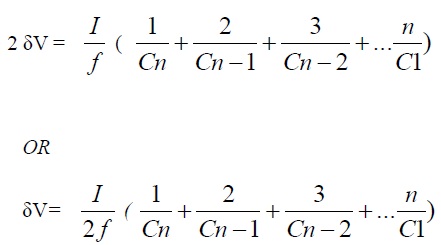
quantity to be evaluated is the voltage drop ΔV which is the difference between the theoretical no load voltage 2nVmax and the onload voltage.
Voltage drop ΔV = (I/fc) (2/3 n³ + n²/2-n/6) 
Regulation of voltage = V/2nEm,
Ripple (%) = δV/2nEm

RIPPLE VOLTAGE
Ripple voltage is the magnitude of fluctuation in DC output voltage at a specific output current (assuming AC input voltage and AC input frequency are constant). A close approximation for series half-wave multipliers can be expressed as:
VRIP = I(N2+N/2)/8FC
Example: Calculate the ripple voltage of a 6 stage multiplier with 1000pF capacitors, 50kHz input frequency (sine wave), 1mA DC output current, 20kV DC output voltage:
VRIP = (1*10-3(62+6/2))/8*50000*(1*10-9))
VRIP = 97.5Vp-p

DESIGN AND TEST SETUP
For the application of various equipment in 8 stages Cockcroft-Walton multiplier designed with a multiplication of peak to peak voltage ie. N * Vmax at a last stages of Cockcroft-Walton multiplier.
 
Fig -2: Block diagram of test setup
A voltage divider is used for deviation of voltage with a very high resistance. The two main components are used in the setup as shown.in figure 2. They are amplifier and 8 stages voltage multiplier. Amplifier is used to amplify the DC input signal and 8 stages Cockcroft-Walton multiplier is used to step up DC voltage into a high voltage at 1KV or 1000 Volt  from 230 V AC voltage which rectified and convert in AC-DC. Voltage adjuster is used to adjust the voltage and amplifier end for supplying to the Cockcroft-Walton multiplier circuit. The operation of a multiplier is to be effectively multiplying the peak to peak voltage by number of stages and convert into high voltage. The voltage at the 1st stage of multiplication is 120V DC. The voltage at the 8th stage of multiplication is 960VDC. In theoretical consideration these values were somewhat reduced because of losses in the diodes, capacitances and leakage currents of the diodes, component tolerances of the diodes and capacitors, etc. The voltage divider in which high value of resistance are use. In the actual prototyped circuit, we used 10 Mohm resistors because of availability in the experiment. Components are used in prototype model Capacitor and Diode in cascade network, and operational amplifier (741). In figure 3. Shows that if the output voltage of a Cockcroft-Walton multiplier is increase according to number of stages. In theoretically at first stages output is 120 peak to peak voltage and at the end of 8 stages the peak to peak voltages is 960 volt. Developed high voltage D.C. Power supply based on Cockcroft-Walton voltage multiplier circuit. This circuit is a unique circuit which is developed for the special applications like field testing of high voltage cables, prime D.C. voltage. Construction of multiplier circuit is simple in nature because, it is cascading of diodes and capacitors which is low cost component this is the advantages of multiplier circuit and it also required less insulation from last stages of the voltage multiplier circuit.
 
Fig -3: Characteristics of output voltage and number of stages

CAPACITOR AND DIODE SELECTION
While designing multiplier and capacitor and diode must be used based on size consideration for expected load current and expected output voltage. Range of capacitor is commonly 1 microfarad to the 250 microfarad, whose voltage rating is usually twice that of actual peak to peak voltage. For example a capacitor which will see a peak voltage of 2Vmax should have a voltage rating of approximately 4Vmax. For selection of diode, parameter must be consider. When the maximum reverse voltage across a diode that is known as peak inverse voltage. This peak reverse voltage are available in each diode therefor for selection of diode rating which is 2 * Vmax for a safety purpose.

CONCLUSION
The Cockcroft-Walton Multiplier surface mount and design in which high voltage generate without use transformer is a beauty of the high voltage Cockcroft-Walton circuit. There for size of the complete high voltage circuit is small and cost is also less. This small size circuit gives high voltage at the end of multiplier circuit. Because of the light weighted circuit it is portable it gives high reliability. Construction of whole circuit is simple and robust in nature. This multiplier circuit is useful for a scientific instrument, TV sets and CRTs, Oscilloscope, x-ray and photomultiplier tubes and field testing of HV cables.

EXPERIMENTAL SETUP
In this experiment used 1 to 250 microfarad capacitor are used and IN 4007 Diode which is cascading in the Cockcroft-Walton multiplier circuit. Digital multimeter which is used to measure the High Voltage at the end of multiplier circuit.
 
Fig -4: Prototype setup of Cockcroft-Walton multiplier circuit

REFERENCES
[1]. D. F. Spencer, R. Aryaeinejad, E. L. Reber," Using the Cockcroft-Walton Voltage Multiplier Design in Handheld Devices”, INEEL/CON-01-01424 PREPRINT October 2001.
[2]. C. K. Dwivedi ,M. B. Daigavane," Multi-purpose low cost DC high voltage generator (60 kV output), using Cockcroft-Walton voltage multiplier circuit‖, International Journal of Science and Technology Education Research Vol. 2(7), pp. 109 - 119, July 2011.
[3]. G.S. Senthil Raaj, G.T. Sundar Rajan," Simulation and Implementation of Single-Phase Single-Stage High Step-Up AC–DC Matrix Converter based of Cockcroft–Walton Voltage Multiplier‖, International Conference on Innovations In Intelligent Instrumentation, Optimization And Signal Processing “ICIIIOSP-2013”
[4]. Cheeru G. suresh, Elizabedh Rajan,Chittesh V.C.,Chinnu G. suresh," Transformless high step-up DC-DC Cockcroft-Wolton multiplier in hybrid system‖, IRF International Conference on 10th August 2014, Cochin, India, ISBN: 978-93-84209-43-8
[5]. Nileena P. Subhash, Ajmal K.A, K. Punnagai Selvi," A High Step-Up Converter Using Transformerless Cockcroft-Walton Voltage Multiplier for a PV System,‖ International Conference on Engineering Technology and Science-(ICETS’14)
[6]. Adinath Jain, Simith E," AC-DC Matrix Converter Based On Cockcroft-Walton Voltage Multiplier‖, IOSR Journal of Engineering (IOSRJEN), Vol. 04, Issue 07 (July. 2014). PP 16-23
[7]. Naidu MS, Kamaraju V (2004),‖High Voltage Engineering‖, Third Edn. McGraw- Hill Company Ltd. pp. 146-156
[8]. C. L. Wadhwa, ―High Voltage Engineering‖.New Age International Publication. pp. 56-63.

Wednesday, 21 December 2016

GENERATION OF HVDC FROM VOLTAGE MULTIPLIER USING MARX GENERATOR

GENERATION OF HVDC FROM VOLTAGE MULTIPLIER USING MARX GENERATOR
ABSTRACT
The Marx Principle was developed by Erwin Otto Marx. Its principle is to generate a high voltage pulse using a number of capacitors in parallel to charge up during the on time and then connected in series to develop higher voltage during the off period. This principle is used to generate voltages in the range of KV’s in real-time for testing the insulation of the electronic appliances like transformers and the insulation of the power carrying lines. This project consists of 4 stages and each stage is made of one MOSFET, two diodes, and one capacitor. MOSFET is used as a switch; diodes are used to charge the capacitor at each stage without power loss. A 555 timer generates pulses for the capacitors to charge in parallel during ON time. During OFF time of the pulses the capacitors are brought in series with the help of MOSFET switches. Finally, number of capacitors used in series (4 in our project) adds up the voltage to approximately 3 (4 capacitors-1 capacitor) times the supply voltage. This system structure gives compactness and easiness to implement the total system.

INTRODUCTION
With the development of solid-state electronics, solid-state devices are becoming more and more suitable for pulsed power application. They could provide the pulsed power systems with compactness, reliability, high repetition rate, and long life time. The rising of pulsed power generators using solid-state devices eliminates limitations of conventional components, and promises pulsed power technology to be widely used in commercial applications. However, solid-state switching devices such as MOSFET available now are only rated up to a few kilo Volts. Most of pulsed power systems demand much higher voltage ratings.

DEVELOPMENT OF MARX GENERATOR
Conventional Marx Generator
The generator capacitance C is to be first charged and then discharged into the wave shaping circuits. A single capacitor C may be used for voltages up to 200 kV. For producing very high voltages, a bank of capacitor are charged in parallel and then discharged in series. The arrangement for charging the capacitors in parallel and then connecting them in series for discharging was originally proposed by Erwin Otto Marx in 1923 as shown in Fig.1. Usually the charging resistance is chosen to limit the charging current to about 50 to 100 mA, and the generator capacitance C is chosen such that the product CRs is about 10s to 1 min. The gap spacing is chosen such that the breakdown voltage of the gap G is greater than the charging voltage V. Thus, all the capacitances are charged to the voltage V in about 1 minute. When the impulse generator is to be discharged, the gaps G are made to spark over simultaneously by some external means. Thus, all the capacitors C get connected in series and discharge into the load capacitance or the test object. The discharge time constant CR1/n (for n stages) will be very small compared to charging time constant CRs which will be few be very small be very small compared to charging time constant CRs which will be few seconds.
 
Fig.1: Conventional Marx Generator
There are some demerits in the conventional Marx circuit as follows:
·        Long charging time because the charging current flows through the charging resistors.
·        Low efficiency because of the same reason mentioned above.
·        Low repetition rate because of the same reason.
·        Few output voltage appearance in charging period because the charging current flows through the charging resistors and a load.
·        Turn-off is impossible because of using the spark gap switches.
·        Short life time of the spark gap switches.
In order to solve these problems, some new Marx circuits are proposed. These new improved circuits use semiconductor switches such as MOS-FETs or IGBTs.

Modern Marx Generator
With the development of solid-state electronics, solid-state devices are becoming more and more suitable for pulsed power application. They could provide the pulsed power systems with compactness, reliability, high repetition rate and long life time. The rising of pulsed power generators using solid-state devices eliminates limitations of conventional components, and promises pulsed power technology to be widely used in commercial applications. However, Solid-state switching devices such as Metal Oxide Semiconductor Field Effect Transistor (MOSFET) available now are only rated up to a few kilo Volts. Previously, it employed spark gaps as switches which are replaced by electronic switches such as (MOSFETs) and resistors as isolator is replaced by diodes. Therefore, Convention Marx generator had drawbacks such as low repetition rate, short life time, inefficiency are eliminated by modern Marx generator as shown in Fig.2.
 
Fig.2: Contemporary Structure of Marx Generator Charge Mode
In this mode, IGBTs are at off-state. As shown in Figure 2, the high frequency transformer T passes the energy to the secondary winds from a generator of high repetition rates sine voltage. Via the large inductor L and diodes D, the capacitors C in parallel are charged by the high voltage (HV) and high frequency rectify bridge. The large inductor acts as a current limiter and cause boost of the voltage of capacitors.

Discharge Mode
In this mode, IGBTs turn on simultaneously. Then they are at on-state and, consequently, the capacitors are linked in series. Thus, the load could acquire a negative high voltage which is the sum of the voltage of capacitors. Via IGBTs, the capacitors discharge their energy to the load. Diodes take place of resistors as the isolator in conventional Marx generator. Capacitors C, inductor L and diode D1 compose of another discharge loop. In this mode, the inductor L isolates high output voltage apart from the rectify bridge. Some demerits of conventional Marx circuit are improved as follows.
·        Relatively short charging time because the charging current flows through the diodes instead of the charging resistors.
·        Relatively high efficiency because of the same reason mentioned above.
·        Relatively high repetition rate because of the same reason.
·        Turn-off is possible because of using the semiconductor switches instead of the spark gap switches.
·        Long life time of the switches.
 
Fig.3: Block Diagram
Primary energy source is taken as a step down AC supply. It is step down to suitable voltage and rectified to get constant DC supply for charging of capacitors. Capacitors are charge storage device. The charging of capacitor takes place as they are parallel connected to the rectifier. When capacitor is having appropriate charge stored in it, switches are used to connect all capacitor in series and discharge of capacitor take place and we get n times of rectifier voltage across the load. Due to various practical constraints, the output voltage is somewhat less than n×V (where n is stages).

CIRCUIT DIAGRAM
A 555 timer is used astable mode, i.e., pin 2 and 6 are shorted and output is connected to base of BC547 Q6. Collector of Q6 is connected to base of Q5. Pin 3 of timer is also connected to base of Q12 which drives Q11. Collector of Q11 is connected to base of Q7, Q8, Q9 and Q10. Collectors of Q7, Q8, Q9 and Q10 are connected to pin 2 of U4, U3, U2, U1 opto-isolator IC resp. pin 1 of U4, U3, U2 and U1 is connected to Vcc. Emitters of Q7, Q8, Q9 and Q10 are grounded.
 
Fig.4: Circuit Diagram
Capacitors C1 to C6 used supply the driving power to the MOSFETs while C1, C2, C4, C6 are used also for storing the charge in parallel mode while Q5 delivers positive pulses through diodes D1 to D4, D5 to D8 and D10-D13. A 555 timer is used in a stable multi-vibrator mode near 50% duty cycle whose ON period delivers the power at point ‘A’ by 2 switching transistors Q5 & Q6. The ON period also switches to other switching transistors Q10 & Q11 which ultimately switch ON Q7 to Q10 which are used for driving the LEDs of the opto-isolators (MCT2E) U1 to U4. The output of the opto-isolators are connected to gate and source of respective MOSFETs which are thus kept switched OFF as their gate and source are at ground potential. During the OFF time period of the timer all the switching transistor Q5, Q6, Q11, Q12,& Q7 to Q10 remain OFF . This causes the capacitors C2, C3, C4 and C6 to start.

DESIGN DETAILS TIMER
• Ton = 0.693 (R1+R2) C = 0.693 (10000+1000) 100*10^-9 = 0.7ms
• Toff = 0.693*R2*C = 0.693*10000*100*10^-9 = 0.6ms
• Duty cycle = Ton/ (Ton + Toff) = 0.7ms/ (0.7ms+0.6ms) = 53.8%

CIRCUIT SPECIFICATIONS
·        C = (Vo*t)/(R) = (48*10^-3)/(3900) = 98.6uF100Uf
·        Capacitor - 47uF/160V, 100uF/35V, 0.1uF
·        Resistors - 1k,10k,3.9k
·        [range(10-100k);max voltage(50-100kV)]
·        MOSFET - IRFZ44
·        Diode - 1N4007
·        Opto-coupler - MCT2E

SIMULATION
The simulation of conventional Marx generator is done to obtain HVDC upto 2kV. The circuit is shown below:
 
Fig.5: Marx circuit

EXPERIMENTAL RESULTS HARDWARE
The input given was 12V for which an output of 30V was obtained due to losses.
 
Fig.6: Hardware Result

SOFTWARE
For an input of 1kV, 2kV output was obtained. The result is shown in Fig.7. The waveforms are shown in Fig.8.
 
Fig.7: Simulation results
 
Fig.8: Waveforms from simulation

CONCLUSION
The simulation gives the idea of HVDC generation i.e., 2kV using sphere gaps. In this study, solid-state devices such as MOSFET and diodes are used in Marx generator to replace of gap switches and resistors. Furthermore, it is reasonable that MOSFET drivers utilize method of self-supplied power. The Marx generator is used to multiply voltage by using MOSFETS. The number of MOSFETS used decides the number of times the voltage should be multiplied. In this study we have used four stages in hardware and the circuit multiplies the input voltage successfully.

REFERENCES
1] Repetitive and High Voltage Marx Generator Using Solid-state Devices: Yifan Wu, Kefu Liu, JianQiu , XiaoXu Liu and Houxiu Xiao Huazhong, University of Science and TechnologyCollege of Electrical and Electronic EngineeringWuhan, 430074, China.
2] Design and Simulation of Unipolar Solid-State Marx Generator: Shreyashi De, 2Bindu. S, Department of Electrical Engineering, Fr. C. Rodrigues Institute of Technology, Sector-9A, Valhi, Navi Mumbai Email:shreyashide06@gmail.com. binduballu@rediffmail.com.
3] Development of MOS-FET Based Marx Generator With Self-Proved Gate Power Tokuchi1,2,3, w. Jiang2, k. Takayama3, t. Arai3, t. Kawakubo3 and t. Adachi3 1pulsed power Japan laboratory ltd., kusatsu, shiga, 525-0027, Japan 2nagaoka university of technology, nagaoka, niigata, 525-0027, Japan 3high energy accelerator research organization (kek), tsukuba, ibaraki 305-0801, Japan.
4] J.H.Kim and M.H.Ryu: “High Voltage Pulse Power Supply Using Marx Generator & Solid-State Switches”, IEEE 32nd Annual Conf. Industrial Electronics Society, IECON, pp.1244-1247, 2005.
5] R.J. Richter Sand and R.J. Adler, “Marx-stacked IGBT modulators for high voltage, high power applications”, High-Voltage Workshop 25th Intern. Power Modulator Symposium, pp.390-393, 2002.

DESIGN OF AN INTELLIGENT AND EFFICIENT LIGHT CONTROL SYSTEM

DESIGN OF AN INTELLIGENT AND
EFFICIENT LIGHT CONTROL SYSTEM
ABSTRACT
Recently, many researches has been carried out to save the energy in many aspects such as producing a device which consumes very less energy or designing a system which helps to reduce the power consumption using the existing devices. In this paper, a room light control system is proposed which is named as light control system (LCS). This proposed system will able to provide the needed light which provides the satisfaction of users and will provide energy saving and management.
In this paper the Lighting Control System and the decision making algorithm, are discussed. As per the algorithm the system will first check any occupant is there in the room. If so then the system will check the intensity of light in the room and if it is low then it will switch on the light. Our proposed system can able to minimize the energy consumed for lighting in a room and can able to provide it efficiently.
Keywords: Lighting Control system, Energy saving, LDR, PIR sensor

INTRODUCTION
Power saving has become a necessary thing in our day to day life. Many conventional powers saving methods such as using electrical devices which consumes very less energy or cutting off the entire power supply for a scheduled time for a particular area are not efficient and there will be a lot discomforts to the users and cost may also increase to use a low power electrical device.
Buildings are responsible for up to 40% of energy usage. Most part of this energy is used mainly for maintaining good lighting such that the workers feel comfortable. Nowadays the newly constructed modernized or automated buildings may have lighting system to improve the comfort of occupants and to save the energy. But there is large number of old buildings which contains the traditional lighting system. To reduce the energy consumption in those types of buildings and to help the owners of that building in terms of saving electricity bill an intelligent and an effective method is discussed in this paper.
Because of advancement in Sensor technology a very cheap and portable methods to measure our surroundings are available.
The amounts of light required to for a good environment to work comfortably in various areas are shown in table 1 which is recommended by CIBSE lighting guides.’
Table 1 Required intensity of light for various environments
 
EXISTING SYSTEM
This section describes about the most commonly used lighting control system used in buildings. Since this method is going to use wireless sensor network it is mandatory to know the operation of existing lighting control system. It can be decided that energy loss is occurred with a lighting system when the lighting system illuminates a light which is an area which is not being used currently at that particular time or when it illuminates a light even though sufficient lighting is available to work.
The most commonly used lighting systems are explained below.

A Switch operated manually:
In this method a user has to switch ON and OFF the required lights. Since the user can switch on and off the lights as per their preferences there is a chance of keeping the lights in on state even though it was not need during that time. This may occur because of carelessness of user and a large amount of power is wasted.
This approach first checks whether any occupants are there in the room or not.
If anybody is there in that room then it checks the intensity of light, if it is enough then it won’t switch on the light otherwise it switch on the light.

By Detecting Occupants:
The lighting system with occupant detection uses passive infrared sensor (PIR).
This PIR sensor detects any movement is present in that particular area. If any movement is there means then this system automatically switches ON the lights. If timers are not used in this type of system means then the lights will be kept in ON state even after the user left the place. Because of this fault also a large amount of energy can be wasted. Then another drawback about this type of system is, it will switch ON the lights when there is an occupant is present in that area. But there is a possibility of enough lighting will be there at that particular time.
This system is not going to check the intensity of light before switching on the lights. Because of this also a large amount of energy can be lost.

PROPOSED SYSTEM
The proposed system overcomes all the drawbacks of existing system. This system takes two things into account before taking any action, namely (1) human presence and (2) intensity of light. The system consists of a PIR sensor (Parallax 555- 28027) and an LDR (NORP 12). The PIR sensor is used to detect whether any occupants are there in that room and LDR is used to detect the intensity of light in that room. Apart from this an algorithm can be implemented in our system which uses both the LDR and PIR sensor to decide whether to switch on the light or not.
 
Fig.1. Setup of proposed system
SYSTEM DESIGN:

4.1 Block diagram:
 
Figure 2 Block Diagram for the proposed system.
This system can be implemented using a PIC 16F877A, a LDR, A PIR sensor and the lights can be controlled by relays.
The LDR sensor will keep on sensing the intensity of light and sends it to the microcontroller. The PIR sensor will send a signal to the microcontroller if there is any occupant in the room. If anybody is present in the room then the microcontroller compares the sensed value of intensity in the room with the value already stored in the microcontroller. If the sensed value is less than the value stored in the microcontroller then the light will be switched on by connecting the relay.

ALGORITHM
Step 1: Start
Step 2: Check whether any occupant is there in the room using PIR sensor.
Step 3: If any Occupants is there means then compare the intensity of light in the room which was sensed by LDR. If nobody was there means then after some time delay again go to step 1.
Step 4: If the sensed intensity is less than the required level, then switch on the light or if it was enough means then after some time delay proceed to step 1.
As per the algorithm our system will first check whether any occupants are there in the room with the help of PIR sensor where the system has been installed. If any occupants are there then it will check the value of light luminance which is sensed through LDR and then the sensed value will be compared with the value stored in the microcontroller, if the value is less than the lights will be switched on or if the sensed value is greater than the stored value then it will wait for some time and again it will from the first.
While checking for occupants if no one is there in the room then the system will wait for some time (delay), which can be programmed in the microcontroller then it will start from the first step.

FLOWCHART

RESULTS
The proposed system has been implemented in a room with four lights each of 40 watts. Since it is normal classroom where evening classes are also conducted the intensity required has been set to 500 lux which was set as the reference level in microcontroller. Before implementing this system, around 800 watts of energy was consumed per day. After implementing this system in that room it has been considerably reduced to 480 Watts. Thus on using this system a large amount of energy can be saved.

CONCLUSION
The proposed system can able to reduce the power consumption to the maximum limit and also this system will help us to keep the working environment in a pleasant and comfortable manner. In this system the number of persons present in the room (Person counter) can be included and also the data transmission from PIR sensor to microcontroller can be implemented through wireless such that the system will become a scalable one in the sense a single system can able to control a large number of rooms.
Apart from these things the system can be upgraded to allow the users to configure the intensity of light in real time.

REFERENCES
[1] CIBSE. Reasoning about naming systems. The Chartered Institution of Building Services Engineers, 2002.
[2] Intelligent Energy Conservation System Design Based on Hybrid Wireless Sensor Network Hung-Cheng Chen Department of Electrical Engineering, National Chin-Yi University of Technology, Taiwan, Teng-Fa Tsao Department of Electrical Engineering, Nan Kai University of Technology, Taiwan , Chun-Liang Hsu Department of Electrical Engineering, St. John’s University, Taiwan IPCSIT vol. 23 (2012).
[3] Evaluation of Energy-Efficiency in Lighting Systems using Sensor Networks Declan T. Delaney, Gregory M.P. O’Hare, and Antonio G. Ruzzelli CLARITY: Centre for Sensor Web Technologies University College Dublin
[4] Intelligent Lighting System Using Wireless Sensor Networks A.A.Nippun Kumaar , Kiran.G ,Sudarshan TSB Department of Computer Science & Engineering, Amrita Vishwa Vidyapeetham, School Of Engineering, Bangalore Campus, India IJASUC Vol.1, No.4, December 2010
[5] Microchip Technology Inc. PIC16F877A Datasheet, RevisionC, 2003.
[7] Datasheet of NORP 12 LDR