Blog Archive

Showing posts with label simulation. Show all posts

Friday, 22 July 2016

SIMULATION OF EXTRA HIGH VOLTAGE LONG TRANSMISSION LINES

SIMULATION OF EXTRA HIGH VOLTAGE LONG TRANSMISSION LINES
ABSTRACT
The electrical power system mainly consists of three principle divisions the generating stations, y he transmission system and the distribution system. The transmission lines are the connecting links between generating station and the distribution system and lead to other power system interconnections. Now a day, we are using Extra High Voltage (EHV) transmission lines for transmission of power between the generating station and distribution system .The main reasons behind it are the construction of super power stations of very large capacities necessities the transmission at high voltage for this we use EHV lines.At high voltages power loss is also reduced because losses are directly proportional to the square of current. The simulation of transmission line using MATLAB helps us to analyze the behaviors and parameters of transmission line under actual conditions. We are simulating a long transmission line and analyze the waveforms at sending and receiving end. The results obtained after simulation are used in the designing of Extra High Voltage Long Transmission Line Model.

INTRODUCTION
Electrical energy is generated in large hydro electric, thermal and nuclear super and super critical power stations these stations are generally situated far away from the load centers. This necessitates an extensive power supply network between the generating station and consumer load. This network may be divided into two parts transmission and distribution the main part of this transmission system. Transmission line transmits bulk electrical power from sending end to receiving end stations without supplying any consumer en route and it can be divided into two parts primary and secondary. The transmission voltage is re 66kV, 110kV, 132kV, 220kV, 400kV and 765kV.
The more the voltages of transmission line the better the performance and efficiency of the system. For this we use high voltage and extra high voltage transmission lines to transmit electrical power from the sending end substations to the receiving end substations. At the receiving end substations the voltage is stepped down to a lower value of 66kV, 33kv or 11kV. The secondary transmission system forms the link between the main receiving end substations and secondary substations. In the transmission line the voltage can vary as much as 10% or even 15% DUE TO variation in loads the transmission line is the main energy corridor in a power system. The performance of a power system is mainly dependent on the performance of the transmission lines in the system. It is necessary to calculate the voltage current and power at any point on the transmission line provided the values at one point are known. We are aware that in 3 phase circuit problem it is sufficient to compute results in one phase and subsequently predict results in the other 2 phases by exploiting the three phase symmetry. Although the lines are not spaces equilaterally and not transposed the resulting asymmetry is slight and the phases are considered to be balanced as such transmission line calculations are also carried out on per phase basis.
The transmission line performance is governed by its four parameters
Series resistance
Series inductance
Shunt capacitance
Shunt conductance
All these parameters are distributed over the length of the line. The insulation of a line us seldom perfect and leakage currents flow over the surface of insulators especially during bad weather this leakage is simulated by shunt conductance. The shunt conductance is in parallel with the system capacitance. Generally the leakage currents are small and the shunt conductance is ignored in calculations.
The transmission line may be classified as short, medium and long. When the length of the line is less than about 80km the effect of shunt capacitance can be ignored and the line is designated as a short line. When the length is between 80 and 250km the shunt capacitance can be considered as lumped and the line is termed as medium length line. Lines more than 250km long require calculation in terms of distributed parameters are knows as ling lines.

Two Port Networks
A pair of terminals at which a signal (voltage or current) may enter or leave is called a port. A network having only one such pair of terminals is called a one port network.
 
Figure 1. Two-port network
A two-port network (or four-terminal network, or quadripole) is an electrical circuit or device with two pairs of terminals. Examples include transistors, filters and matching networks. The analysis of two-port networks was pioneered in the 1920s by Franz Breisig, a German mathematician.
A two-port network basically consists in isolating either a complete circuit or part of it and finding its characteristic parameters. Once this is done, the isolated part of the circuit becomes a "black box" with a set of distinctive properties, enabling us to abstract away its specific physical buildup, thus simplifying analysis. Any circuit can be transformed into a two-port network provided that it does not contain an independent source.
A two-port network is represented by four external variables: voltage and current at the input port, and voltage and current at the output port, so that the two-port network can be treated as a black box modeled by the relationships between the four variables Vs, Is, Vr and Ir. There exist six different ways to describe the relationships between these variables, depending on which two of the four variables are given, while the other two can always be derived.
Note: All voltages and currents below are complex variables and represented by phasors containing both magnitude and phase angle.
The parameters used in order to describe a two-port network are the following: Z, Y, A, h and g. They are usually expressed in matrix notation and they establish relations between the following parameters:
(1)Input voltage V1
(2) Output voltage V2
(3) Input current I1
(4) Output current I2

ABCD Parameters
 
Figure 2.transmission network
Two port representation of a transmission network.
Consider the power system shown above. In this the sending and receiving end voltages are denoted by VS and VR respectively. Also the currents IS and IR are entering and leaving the network respectively. The sending end voltage and current are then defined in terms of the ABCD parameters as
So,
This implies that A is the ratio of sending end voltage to the open circuit receiving end voltage. This quantity is dimension less. Similarly,
 
i.e., B , given in Ohm, is the ratio of sending end voltage and short circuit receiving end current. In a similar way we can also define
 
Also,
The parameter D is dimension less.
Note: Here A and D are dimensionless coefficients, B is impedance andC is admittance. A negative sign is added to the output current I2in the model, so that the direction of the current is out-ward, for easy analysis of a cascade of multiple network models.

SIMULATION
Various blocks used
Resistor
The Resistor block models a linear resistor, described with the following equation:
Where,
V Voltage
I Current
R Resistance
Connections + and – are conserving electrical ports corresponding to the positive and negative terminals of the resistor, respectively. By convention, the voltage across the resistor is given by V(+) – V(–), and the sign of the current is positive when flowing through the device from the positive to the negative terminal. This convention ensures that the power absorbed by a resistor is always positive.

Capacitor
The Capacitor block models a linear capacitor, described with the following equation:
Where,
I Current
V Voltage
C Capacitance
t Time

Inductor
The Inductor block models a linear inductor, described with the following equation:
Where,
I Current
V Voltage
L Inductance
t Time

Voltage Sensor
The Voltage Sensor block represents an ideal voltage sensor, that is, a device that converts voltage measured between two points of an electrical circuit into a physical signal proportional to the voltage.

Voltage Measurement
The Voltage Measurement block measures the instantaneous voltage between two electric nodes. The output provides a Simulink signal that can be used by other Simulink blocks.

AC Voltage Source
The AC Voltage Source block implements an ideal AC voltage source. The generated voltage is described by the following relationship:
Negative values are allowed for amplitude and phase. A frequency of 0 and phase equal to 90 degrees specify a DC voltage source. Negative frequency is not allowed; otherwise the software signals an error, and the block displays a question mark in the block icon.

Scope
The Scope block displays its input with respect to simulation time.
The Scope block can have multiple axes (one per port) and all axes have a common time range with independent y-axes. The Scope block allows you to adjust the amount of time and the range of input values displayed. You can move and resize the Scope window and you can modify the Scope's parameter values during the simulation.

Solver Configuration
Each physical device represented by a connected Simscap block diagram requires global environment information for simulation. The Solver Configuration block specifies this global information and provides parameters for the solver that your model needs before you can begin simulation.
Each topologically distinct Simscape block diagram requires exactly one Solver Configuration block to be connected to it.

Breaker
The Breaker block implements a circuit breaker where the opening and closing times can be controlled either from an external Simulink signal (external control mode), or from an internal control timer (internal control mode).

Ground
The Ground block implements a connection to the ground.

Add
The Add block performs addition or subtraction on its inputs. This block can add or subtract scalar, vector, or matrix inputs. It can also collapse the elements of a signal.

Sine Wave
The Sine Wave block provides a sinusoid. The block can operate in either time-based or sample-based mode.

Fcn Block
The Fcn block applies the specified mathematical expression to its input. The expression can be made up of one or more of these components:
  • u - The input to the block. If u is a vector, u(i) represents the ith element of the vector; u(1) or u alone represents the first element.
  • numeric constants
  • Arithmetic operators (+ - * /^)
  • Relational operators (== != ><>= <=) — The expression returns 1 if the relation is true; otherwise, it returns 0.
  • Logical operators (&& || !)-The expression returns 1 if the relation is true; otherwise, it returns 0.
  • Parentheses
  • Mathematical functions — abs, cos, sin, exp, log, pow, tan, sinh, sqrt etc.
  • Workspace variables — Variable names that are not recognized in the preceding list of items are passed to MATLAB for evaluation.

PI Section Line
The PI Section Line block implements a single-phase transmission line with parameters lumped in PI sections. For a transmission line, the resistance, inductance, and capacitance are uniformly distributed along the line. An approximate model of the distributed parameter line is obtained by cascading several identical PI sections, as shown in the following figure.
Unlike the Distributed Parameter Line block, which has an infinite number of states, the PI section linear model has a finite number of states that permit you to compute a linear state-space model. The number of sections to be used depends on the frequency range to be represented.

PS Simulink Converter
The PS-Simulink Converter block converts a physical signal into a Simulink output signal. Use this block to connect outputs of a Physical Network diagram to Simulink scopes or other Simulink blocks.
The Output signal unit parameter lets you specify the desired units for the output signal. These units must be commensurate with the units of the input physical signal coming into the block. The Simulink output signal is unitless, but if you specify a desired output unit, the block applies a gain equal to the conversion factor before outputting the Simulink signal. For example, if the input physical signal coming into the block is displacement, in meters, and you set Output signal unit to mm, the block multiplies the value of the input signal by 10e3 before outputting it.

Display
The Display block shows the value of its input on its icon. You control the display format using the Format parameter:
  • short - displays a 5-digit scaled value with fixed decimal point
  • long - displays a 15-digit scaled value with fixed decimal point
  • short_e - displays a 5-digit value with a floating decimal point
  • long_e - displays a 16-digit value with a floating decimal point
  • bank - displays a value in fixed dollars and cents format (but with no $ or commas)
  • hex (Stored Integer) - displays the stored integer value of a fixed-point input in hexadecimal format
  • binary (Stored Integer) - displays the stored integer value of a fixed-point input in binary format
  • decimal (Stored Integer) - displays the stored integer value of a fixed-point input in decimal format
  • octal (Stored Integer) - displays the stored integer value of a fixed-point input in octal format

First Simulation Model
In this we tried to implement the simulation of the transmission line by using its equivalent diagram.
 
Figure 3.first simulation model
Although there were no errors but the simulation was not showing desired results. There was also no consideration of length and solver configuration block was not implemented correctly.

Second Simulation Model
Consider the standard model1 of a transmission line (Fig. 4).
 
Figure 4. standard model of transmission line
Both the voltages and the currents can be separately analyzed using Kirchhoff‘s laws and put in terms that can be analyzed using Simulink. Let’s analyze the model, writing all time-based variable sin the transmission line in terms of the Laplace transform variable, s. The spatial variation of the transmission line will be in corporated into the discrete section number:
For the simulation of the voltage response of the transmission line, the voltageV1 across the capacitor in the first loop (which includes the voltage source in Fig.4) can be written in terms of the voltage source, Vs, and the voltage in the second loop V2 as
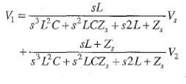
(1) 
Where, Zsis the source impedance. In the transmission line, the elements L and C are the inductance per unit length, and the capacitance per unit length, respectively. The voltage across the capacitor in an Intermediate loop, n, can be written in terms of the similar voltage Vn-1 in the previous loop (n-l), and the voltage Vn+1 in the following loop (n+1).
(2)
A load impedance, ZL, is in parallel with the capacitor in the final loop, k. The load impedance can be linear or nonlinear.
We define the current in the load impedance at the end node, k, via the relation
(3)
Where g( Vk) is an arbitrary nonlinear function that has to be specified by the simulator. In the linear case, g(Vk) is equal to a constant multiplied by V(Fig. 5). From Fig. 5, we find the voltage Vk to be
(4)
 
Figure 5.simulink simulation of the voltage response of the transmission line
For purposes of simulating the current response of the transmission line, the current in the first loop (which includes the voltage source in Fig. 4) can be written in terms of the voltage source V, and the current in the second loop i2.
(5)
The current in an intermediate loop, n can be written in terms of the current in the previous loop (n-1) and the following loop (n+1):
(6)
For the case of linear load impedance, i =V/ZL, the load impedance ZL is in parallel with the capacitor in the final loop, k. The current in this loop is written in terms of the current in the previous loop (k-1)
(7)
Equations 5-7 determine the elements of a second transmission line. In Fig, 5, the critical Simulink elements are shown for the elements specified with Equations 1-4. A dialog menu with Simulink allows all parameters of the polynomial to be specified. We specify the voltage source, Vs, as a half sine wave generator, which acts as a pulse generator in the simulation. The amplitude and width were controllable parameters. In our application, fifteen identical intermediate elements were used. Although we will use only a Limited number of sections in our transmission line model, it can be generalized to include as many as desired.
In addition, the user can specify numerical values for the circuit elements L, C, Zs, and ZL. For clarity of presentation, we include as equentially increasing “dc offset” to each section. Both linear [ik=g(Vk) = constant*Vk] and nonlinear [ik=g(Vk)] load impedancesare described with this model.
 
Figure 6.matlab simulation model
MATLAB simulation model
But there were two major problems that we were unable to solve First of all there was no reference to the length of line.
Second the type of function to be used was unknown.

Third Simulation Model
In this we have used a PI Section Line and specifies all the required parameters of the transmission line like R,C,L and Length. We have also made the required connections with the scope so that input and output voltages can be calculated.

Waveforms obtained at the scope block after the completion of simulation.

CONCLUSION
By the study and simulation of Extra High Voltage Transmission lines we have come to the conclusion that they are best suited for transmission of bulk power.
REFERENCES
(1) Circuit Analysis by A.Chakraborthy
(2) IEEE paper by “Karl E. Lonngren and Er-Wei Bai” on Simulink Simulation of Transmission Line”
(3) MATLAB book (name to be given)
(4) Power System Analysis And Design by B.R.Gupta

Tuesday, 10 May 2016

DESIGN, IMPLEMENTATION AND PERFORMANCE STUDY OF PROGRAMMABLE AUTOMATIC VOLTAGE REGULATOR

DESIGN, IMPLEMENTATION AND PERFORMANCE STUDY OF PROGRAMMABLE AUTOMATIC VOLTAGE REGULATOR

ABSTRACT

This paper proposes the design and implementation of a Programmable Automatic Voltage Regulator (PAVR) with higher precision, appropriate hysteresis and defense of anomaly. Current systems available locally lack precision and suffer the problem of oscillating between two output voltage and hence creating surge at the output which can damage valuable electronics. To avoid these, the stabilization of power voltage, minimization of output wave rate and unchangeable power-voltage to the instruments are needed while the load changes. That requires the maintenance of stable voltage and rapid reaction against the sudden change of input voltage and load. This paper defines the shortcomings and introduces a new system in the tolerable and substantial stable of 220V with '4.5% output accuracy for any deviation of input supply voltage within 100V-340V. To control the whole system automatically a microcontroller is used with some protection devices where to detect fault and the circuit implementation in this system are simple and flexible than conventional analog control circuitry. A simulation for both circuit and program has been accomplished for establishing better performance.
Keywords: Programmable Automatic Voltage Regulator (PAVR), Hysteresis, Microcontroller, Protection, Simulation.

INTRODUCTION
AC power supply by Power Development Board (PDB) in Bangladesh is subjected to variation from time to time. Moreover in rural areas supply voltage remains lower than specified most of the times. This poses a considerable threat to the sophisticated electronic devices. For that reason, many important electric machine or electric equipments may destroy. Power quality related problems, in particular voltage sags, surge and brownouts have a major negative impact on industrial productivity. This appears to be true for both industrialized as well as developing nations. So ensuring the input voltage to remain in a tolerable pre-specified limit has become a necessity in rural as well as some urban areas. In order to save these we need to use the Automatic Voltage Regulator.
An AVR is an electronic device that automatically regulates a variation of input voltage at a certain desired level to load. The voltage of main power supply may be affected by various troubling physical factors, so that special regulating equipment is required to keep the voltage steady. In replace of AVR, Programmable AVR is more flexible, easy to modify and the best for good precision and hysteresis. The existing systems like servo-stabilizers, CVTs, Ferro resonant regulators, thyristor ac regulators, tap changers and the electronic regulators are the available means for voltage regulator. Here the performances of existing commercially available technologies are compared by this system regarding response, faults handling, precision, efficiency and other important parameters. It is essential that the supply ac voltage is needed to operate automatically due to the interconnections among the systems in modern age. The electronic control circuit may be utilized to get the desired output which is very simple, flexible, reliable and cost effective.
AVR mainly functions to measure and regulate the input voltage for producing the stable output and to provide the Protection against sag, surge, spike, impulse, notch, brown out, over voltage, under voltage, over current and hysteresis to the sophisticated equipments and machineries. In this system, the whole operations are implemented by a microcontroller. Microcontroller here performs all actions in accordance with the program maintaining proper precision and hysteresis as we desire and the undesired input transitions are handled by the AC protection devices. The whole proposed design is illustrated in the following block diagram (Figure-1).
 
Figure-1: Block diagram of PAVR
A multi-tapped transformer with input supply and switches connected in primary and in secondary respectively to obtain regulated and stabilized output voltage at the load side is used. Here microcontroller plays the important role to decide and hence to control the switches through which secondary tap carries the power from input to load with a steady voltage. This system also provides the protection against surge, spike, lightning, overvoltage and excess current by adding AC breaker (MCB), Automatic Voltage Switcher (AVS) [25] in the Input line. In the upcoming sections the designing procedure with simulations, programming, the control operation of microcontroller and performance analysis will be discussed.

DESIGNING PROCEDURE AND DISCUSSION
Description of Circuit Design
As the designing commitment which is to stabilize automatically a large range (100V- 340V) variation of input voltage at a normal prescribed level output voltage (Table-1) with a great precision. For this the voltage regulation of input supply is designed which is regulated automatically in such a way that when the input voltage varies, the output voltage will remain stable at a constant value. To achieve this, a microcontroller has been programmed is such a way that when the dc input to microcontroller varies in accordance with the variation of input voltage, microcontroller will operate the suitable switch to get a regulated output from desired transformer tap. Table-1 represents the designing configuration of the multi-tapped transformer.
Firstly, the microcontroller compares a converted variable DC voltage which is found by stepped down the ac supply voltage with the range, which is shown in Table-2 and is set in the memory of the microcontroller. The voltage range for the program has been chosen in such different manner for letting switches functioned to select the different taps for getting desired output of around 220V AC (Table-2). Thus the stable output voltage occurs at the output of this designed regulation system for any short of variation of input voltage automatically. The whole schematic of the PAVR is shown in Figure-2 and Figure-3.
 
Figure-2: Schematic diagram of PAVR (Part-1)
 
Figure-3: Schematic diagram of PAVR (Part-2)

Simulation Procedure
To determine the accurate level of voltage for designing of switching and making the microcontroller program this circuit has been simulated using PSPICE Simulator. The operation of switching of PAVR at different level of input voltage is observed as well. Here, for input supply voltage of 130V, the switching operation is shown graphically in
Figure-4 where the switch under PB0 and Q0 is “ON”. At any input voltage within 100V- 340V, one and only one switch is activated at a time as defined in the program.
 
Figure-4: Simulation for 130V Input

Flowchart description
The microcontroller program of the PAVR is designed and functioned, as the following flowchart (Figure-5), to measure the received DC voltage and then to compare with the prescribed range stored in the microcontroller memory and finally to obtain a decision for the output. In the flowchart, it is also shown that when the received DC input is out of the range (i.e. above 5V and below 1V), microcontroller will operate “No Operation (NOP)”. That means, the PAVR will remain “OFF” during excess high and low voltage AC supply to protect the devices and equipments from damaging. Here the increasing and decreasing of DC input voltage are given orderly to maintain the hysteresis properly.
 
Figure-5: Flowchart for the program of microcontroller operation

Description of Program Operation
The program that was designed for the PAVR has been simulated using PIC Simulator IDE software [28]. PIC Simulator IDE is a basic complier, assembler, disassembler and debugger for microchip family PICmicro. Firstly, the microcontroller has to be selected to load the program. Then the simulation has to be run. The sequences of operation have to be executed as follows.
Option>Select Microcontroller
Tools>Assembler
File>open/PAVR.asm
Tools>Assemble & Load
Simulation>Start
Tools>Microcontroller View
Tools>8×LED Board
The overview of simulation is presented by Figure-6 with PIC Simulator IDE interface. In this figure, the PORTB0 is displayed as ON when the input voltage is in the range of 1.0V-1.5V (2Ch-0Fh).
 
Figure-6: The simulation interface of PIC Simulator IDE with output Display

Description of Microcontroller Operation
A PIC16F876A CMOS FLASH-based 8-bit microcontroller (Figure-7) is used to control the whole system which is more reliable, simple and flexible than conventional analog control circuitry. It features especially Self-reprogrammable under software control, 2 I/O pins & 3 I/O ports, 256 bytes of EEPROM data memory, 2 Comparators, 5 channels of 10-bit Analog-to-Digital (A/D) converter, Programmable code protection, Power-saving Sleep mode, Selectable oscillator options and In-Circuit Debug via two pins.
 
Figure-7: Pin diagram of PIC16F876A Microcontroller with program placing.
An assembly language program is loaded in the microcontroller memory (Figure-7) that configures the A/D module, comparator module and I/O ports, and sets different registers of the memory with the different range of digital code (Table-3). In the program the registers are assigned by any arbitrary names to make the program more readable.
Here port-A is used as input port and port-B as output port. Firstly, microcontroller receives the DC input corresponding to supply AC input from stepped-down transformer at RA1 of PORTA. And then it is compared with the ranges that are set in the memory of microcontroller in the form of code via an A/D converter and a comparator. After that it makes anyone of the output pins (RB0-RB7) of PORTB HIGH corresponding to the range, as mentioned in Table-2, which in turn activates a respective switch to get the regulated output from the transformer. Here a constant voltage level is maintained although the input voltage level goes high than the constant desired level (Table-4). To sense this change, the microcontroller periodically checks terminal voltage and compares this with defined reference voltage levels. For designing purpose the reference voltage and code as a range has been calculated to corresponding pins of PORTB. This is shown in Table-2 and Table-3.
Table-1: (For the Design of Multi-tapped Transformer) Output Voltage Range corresponding to Input Range and Transformation Ratio at different Taps at Normal Input Voltage of 220V
Table-2: Selection of output pins, Switches and Transformer Taps for the prescribed input DC voltage range corresponding to input AC supply voltage range.
Table-3: Hexadecimal Value of digital code equivalent to prescribed DC voltage range corresponding to AC input and PAVR output voltage.
Table-4: Experimented Analog DC input for ADC of Microcontroller and Regulated AC Output Voltage for typical AC Input Supply

PERFORMANCE ANALYSIS
This system has been experimented practically after designing. Here for some typical AC input voltage supply, the regulated output approximate to desired level is found that is shown in Table-4. From this table, it is clearly revealed that this PAVR is able to regulate any variation of input voltage of a system within 100V-340V at a stable range of 210V- 230V and also to defend the system from damage due to extreme decrease and increase in AC supply voltage which is out of the range of 100V-340V. In Figures below present some performance curves of PAVR. Figure-8 shows the desired response curve of PAVR which is produced from the desired output voltage (210V-230V) for any input supply voltage within range of 100V-340V. In Figure-9, a typical input-output voltage characteristics curve of PAVR is put on view of the regulated output voltage that is near about 220V AC (Data in Table-4).
The Figure-10 exhibits a practical input-output voltage characteristics of PAVR for random supply. In this response curve, it confirms the design requisition of a stable output in range of 210V-230V as the regulation of any change in AC supply voltage within 100V- 340V, and the protection any system from spoiling due to low voltage i.e. below 100V and high voltage i.e. above 340V. A hysteresis curve, given in Figure-11, shows the hysteresis behavior of PAVR during the operation of switches at the transition of different ranges of input supply voltage. It is needed to maintain properly to prevent the frequent vacillation of switching between “ON” and “OFF”.
 
Figure-8: Desired Response Curve of PAVR

 
Figure-9: Typical Input-Output Voltage Charactesistics of PAVR

 
Figure-10: Practical Input-Output Voltage Characteristics of PAVR for Random Supply

 
 Figure-11: Hyteresis Curve
CONCLUSION
It is clear that, from above design and discussion, and the comparison shown in Table-5 with some other common existing AVR systems, my proposed proprietary PAVR performs better than any other existing systems. Because it is mainly programmable that can be programmed as the demand maintaining proper precision and sufficient hysteresis over a wide range of input variation. Here the protection against the excessive high and low voltage and current is confirmed which is crucial for the sophisticated electrical and electronic equipments. It is mentionable that the PAVR is very much cheap than other systems because of having microcontroller in place of discrete electronic components and simple protection units. Therefore, the circuit design and implementation are very much easy, flexible and the efficiency of this system is good enough as well. According to market comparison study, the commercially available AVR has a three to four step stabilization of the input variable voltage where the output becomes a big changing stable value within a prescribed range that is not an absolute design to get an output precised. For this reason in my research the way has been adopt to make the system for getting the precision output within in a large variation of input is the design of the main transformer having a many number of taps in the secondary winding side of the transformer maintaining a small turn difference between two adjacent taps. PAVR is applied to all electrical and electronics equipments especially in communications and precision instruments of manufactories.

REFERENCES
[1] WD. Stevenson, Elements of Power System Analysis, McGraw-Hill International, Singapore, Fourth Edition, pp. 337-341, 354-365, 1983.
[2] J. Lamoree, D. Mueller, P. Vinett & W. Jones, Voltage sag analysis case studies, IEEE Transactions on Industry Applications, vol. 30 pp. 1083-1089, 1994.
[3] VK. Mehta & R. Mehta, Principles of Power System, S. Chand & Co., New Delhi, Third Edition, 2003.
[4] FD. Martzloff, Coordination of Surge Protectors in Low-Voltage AC Power Circuits, IEEE Transactions on Power Apparatus and Systems, vol. 99, pp. 129-133, 1980.
[5] MM. Hoque & AI. Mahmod, An Improved Automatic Voltage Regulation System with Apposite Hysteresis and Immense Precision, Chittagong University Journal of Science, vol. 33, pp. 21-33, 2010.
[6] M. Rasheduzzaman, MM. Hoque, NK. Das & JP. Chakrabartty, Design and implementation of an automatic voltage regulator (for ceiling fan) using temperature sensor, G-Science Implementation and Publication, International Online Journal of Engineering, vol. 5, pp. 207-
211, 2008.
[7] BL. Theraja, AK. Theraja, A text book of Electrical Technology, S. Chand & Co., New Delhi, 23rd Edition, pp. 335-338, 1029-1035 & 1098-1104, 2002.
[8] AP. Malvino, Electronic principles, McGraw-Hill International, Singapore, Sixth Edition, pp. 815-826, 1999.
[9] J. Millman & CC. Halkias, Integrated Electronics, Analog and Digital Circuit and System, Tata Mcgraw-Hill Edition, pp.568-470 & 583-585, 1991.
[10] GK. Mithal & M. Gupta, Industrial and Power Electronics, Khanna Publishers, India, Nineteenth Edition, pp. 79-90, 2003.
[11] CT. Pan & TY. Chang, An improved hysteresis current controller for reducing switching frequency. IEEE Transactions on Power Electronics, vol. 9, pp. 97-104, 1994.
[12] V. Sudha & M. Krishnaveni, Power fluctuations-usage of servo voltage stabilizers in industries, International Journal of Applied Engineering Research, Dindigul, vol. 2, pp. 283-289, 2011.
[13] D. Hou & J. Roberts, Capacitive voltage transformer: transient overreach concerns and solutions for distance relaying, Canadian Conference on Electrical and Computer Engineering, vol. 1, pp. 119 – 125, 1996.
[14] H. Hart & R. Kakalec, The derivation and application of design equations for ferroresonant voltage regulators and regulated rectifiers, IEEE Transactions on Magnetics, vol. 7, pp. 205- 211, 1971.
[15] MC. Huang, J. Lu & YJ. Peng, Research on Trigger Methods for Thyristor AC-Voltage Regulator, Journal on Power Electronics, vol. 02, 2004.
[16] DH. Jang, Chungnam & GH. Choe, Step-up/down AC voltage regulator using transformer with tap changer and PWM AC chopper, IEEE Transactions on Industrial Electronics, vol. 45, pp. 905-911, 1998.
[17] DL. Fletcher & WO. Stadlin, Transformer Tap-Position Estimation. Proceedings, 13th PICA Conference, pp.226 -232, 1983.
[18] MS. Calovic, Modeling and Analysis of Under-Load Tap-Changing Transformer Control Systems, IEEE Transactions on Power Apparatus and Systems, vol. 103, pp. 1909-1915, 1984.
[19] JA. Jindrick & K. Nohria, Microprocessor Based Control of Transformer Tap- Changing, McGraw-Edison Bulletin 82016. 1982.
[20] N. Kutkut, R. Schneider, T. Grant & D. Divan, AC voltage regulation Technologies, Power Quality Assurance, pp. 92 -97, 1997.
[21] KE. Addoweesh & AL. Mohamadein, Microprocessor based harmonic elimination in chopper type AC voltage regulators, IEEE Transactions on Power Electronics, vol. 5, pp. 191-200, 1990.
[22] PIC16F876A, 28/40/44-Pin Enhanced Flash Microcontrollers Data Sheet, Microchip Technology Incorporated, ISO 9001/ QS-9000. U.S.A. 2003.
[23] Miniature Circuit Breakers and Switches, Class 720, QOU, Schneider Electric USA, 0720CT9401R1/05, 2005, available at http://www.uecorp.com/busway/faq_pdf/ qou.pdf
[24] W Breer, P Hug, U Hunziker, R Kaltenrieder, H Unterweger & H Weichert, Low-Voltage Switchgear and Controlgear, Allen Bradley - Rockwell Automation, Milwaukee, USA, 2009
[25] V Sukumar & T Castagnet, An Automatic Line Voltage Switching Circuit, AVS10-30, SGSTHOMSON Microelectronics, 1995
[26] Berkley Spice, SPICE8, Electrical and Electronic Simulation Software, 1970.
[27] RL. Boylsted & L. Nashelsky, Electronic Devices and Circuit Theory, Prentice-Hall, USA, 6th Edition, pp.741-748 & 773-780, 1996.
[28] Vladimir Soso, PIC Simulator IDE v.6 91, Oshon Software, 2011.
[29] Configuration of Automatic Voltage Regulator, SAMSUNG, VENUS, MICROTECH, VENSTAB, SILICON.